


Materials Science & Semiconductors via Novel Materials
As we continue to push the limits of computing power and speed, the need for advanced semiconductor design becomes increasingly important. While traditional silicon-based chips have served us well in the past, they are reaching their limits in terms of performance and energy efficiency. The solution? Novel materials.
By incorporating new materials into semiconductor design, we can create next-generation chips that are faster, more powerful, and more energy-efficient than ever before. This is where materials science comes in.
In this article, we’ll explore how researchers are creating next-generation chips with novel materials.
What is Materials Science?
Materials science is the study of the properties and behavior of materials. It allows us to design and engineer materials with specific properties, such as conductivity, thermal stability, and durability. By combining this knowledge with semiconductor design, we can create chips that are tailor-made for specific applications.
Creating Next-Generation Chips with Graphene
One example of a novel material that is being used in semiconductor design is graphene. Graphene is a two-dimensional material that is made up of a single layer of carbon atoms. It has exceptional electrical and thermal conductivity, as well as remarkable strength and flexibility.
Graphene is being incorporated into semiconductor design in a number of ways. One approach is to use graphene as a replacement for traditional metal interconnects. Metal interconnects can become a bottleneck for performance as chips become more complex, but graphene interconnects can provide faster and more efficient connections between different parts of a chip.
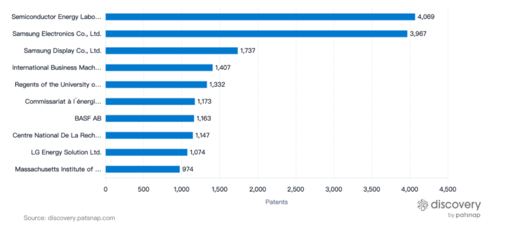
Samsung Electronics and IBM continue to lead the way in graphene technology, as shown above. As a highly sought-after material, graphene has numerous applications across industries, from electronics to energy. With their impressive track record in graphene innovation, it’s hardly surprising that Samsung and IBM continue to dominate in this space.
Creating Next-Generation Chips with Molybdenum Disulfide
Another example of a novel material being used in semiconductor design is molybdenum disulfide (MoS2). MoS2 is a two-dimensional material that is a semiconductor, meaning it can be used to control the flow of electrical current. MoS2 has a number of advantages over traditional silicon, including higher electron mobility and better performance at high temperatures.
MoS2 is being used in a variety of applications, including transistors and photovoltaic cells. By using MoS2 instead of silicon in these applications, we can create devices that are more energy-efficient and have better performance.
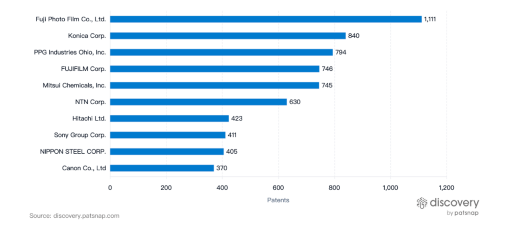
The MoS2 technology space has some unexpected leaders when it comes to patent filings. It turns out that Fuji Photo Film and Konica are at the forefront of MoS2 innovation, followed closely by Hitachi, Sony, and Canon.
Other Novel Materials for Semiconductor Design
In addition to graphene and MoS2, there are a number of other novel materials being used in semiconductor design. These include gallium nitride (GaN), indium gallium arsenide (InGaAs), and perovskite materials.
GaN is a wide-bandgap semiconductor that has a number of advantages over traditional silicon, including higher efficiency and better power handling capabilities. GaN is being used in a variety of applications, including power electronics and LED lighting.
InGaAs is a semiconductor material that has a higher electron mobility than silicon. This makes it well-suited for use in high-speed transistors and other high-performance devices.
Perovskite materials are a class of materials that have a unique crystal structure. They are being investigated for use in solar cells, as they have the potential to be much cheaper and more efficient than traditional silicon-based solar cells.
By incorporating these novel materials into semiconductor design, we can create next-generation chips that are faster, more powerful, and more energy-efficient than ever before. This is an exciting time for materials science and semiconductor design, and we can expect to see many more breakthroughs in the years to come.
Your recommended content
-
All Charged Up: Power Batteries & The Patent Race Shaping the Future of Electric Mobility
Category: Article | Category: battery technology | Category: electric vehicle | Category: EV | Category: lithium ion | Category: lithium ion battery | Category: NEV | Category: new energy vehicles
Monday, April 22, 2024
In the ever-evolving landscape of innovation, the electric vehicle (EV) industry stands as a beacon of technological transformation. As nations...
-

The People vs. AI: Who Owns Ideas in the Era of Generative Artificial Intelligence?
Category: AI era | Category: AI-driven creativity | Category: AI-generated creations | Category: Article | Category: copyright and patent rights | Category: digital innovation | Category: innovation | Category: intellectual property law | Category: legal implications | Category: OpenAI Sora | Category: patent law | Category: Research Tag | Category: Sora | Category: text-to-video generative AI | Category: who owns AI
Monday, April 22, 2024
In the ever-evolving landscape of technological innovation, OpenAI's Sora emerges as a groundbreaking force, blurring the lines between human creativity and artificial intelligence. As the forefront of text-to-video generative AI, Sora's capabilities have ignited profound discussions around copyright and patent rights, challenging established legal frameworks and prompting a reevaluation of intellectual property rights in the digital age. With its capacity to generate high-quality footage based on mere prompts, Sora exemplifies the potential of AI-driven creativity, yet it also raises complex ownership dilemmas and ethical considerations. As we navigate this uncharted territory, it becomes imperative to explore the intersection of intellectual property law and AI technology, deciphering the legal challenges and implications posed by AI-generated creations. From the nuances of copyright law to the ethical dimensions of AI development, this editorial delves into the multifaceted landscape of Sora's impact, offering insights into the future of innovation and ownership in the AI era.
-

Patsnap Releases 2023 Global Innovation Report: The Brilliant Names to the Dynamic Landscape of Innovation
Category: Article | Category: eBook | Category: Research Tag | Category: Whitepaper
Wednesday, November 15, 2023
The Global Innovation 100 and Global Disruption 50 transcend individual entities, each representing a small innovation ecosystem with numerous subsidiaries. Through the innovation data of these companies, we gain insights into the characteristics, structures, and trends of global innovation.